

Earth’s thinnest material may offer ‘amazing’ value for Information Age
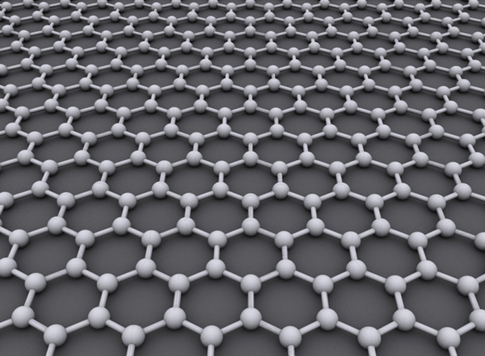
It’s known as the thinnest material on Earth and one you can find in something as everyday as a pencil: graphene.
In 2010, Manchester researchers Andre Geim and Kostya Novoselov won a Nobel Prize in Physics with it just six years after they discovered how to isolate a single atomic layer of it quite unceremoniously – by repeatedly applying Scotch tape to increasingly thinner flakes of graphite that started as a pencil-drawn line until they ended up with just one monolayer of the multipurpose carbon atoms.
“You could have done this Nobel-worthy research, too, if you only knew what to look for and, most importantly, believed that isolating a single atomic layer of any substance is possible, which almost nobody believed at that time,” said Texas A&M University theoretical physicist Alexey Belyanin, a member of the Department of Physics and Astronomy and George P. and Cynthia Woods Mitchell Institute for Fundamental Physics and Astronomy. “The Nobel Museum in Stockholm collects artifacts of Nobel discoveries donated by Nobel laureates. There, among pieces of complicated apparatuses, you can find Scotch tape and a chunk of graphite donated by Kostya Novoselov as a joke. Playfulness has always been one of the hallmarks of Geim-Novoselov team.”
Although graphene has been isolated 15 years ago, many of its properties still remain unknown or unexplained, especially on ultrafast scale. For the past several years, Belyanin has been working to change that in collaboration with University of Colorado experimental physicist Markus Raschke. Using an optical imaging technique developed by Raschke, the two research groups recently obtained an unprecedentedly up-close look at graphene, exploring its properties at a resolution of only a few nanometers — about 100 times better than a standard optical microscope that is limited by wavelength of light, enabling them to follow the motion of atoms and electrons in the material on a scale of just a few femtoseconds.
Their work, detailed in a paper published this summer in Nature Nanotechnology and highlighted in a related News & Views article, provides new insight into how graphene interacts with light – specifically, how its electrons respond to intense optical excitation at the nanoscale and with femtosecond time resolution. This invaluable information stands to play an important role in the design of future nanophotonic devices based on graphene and other two-dimensional materials used in computers and telecommunications.
“Graphene is an amazing material for our Information Age,” Belyanin said. “It conducts electricity like a metal, but it is almost completely transparent, so it can be used as a transparent contact in smart displays, lasers and other optoelectronic devices. You can make atomically flat transistors, waveguides, modulators or detectors of light out of graphene for future integrated photonic circuits.”
The team achieved their unprecedented detail by bringing a 10-nanometer gold tip a few nanometers from the graphene’s surface, then illuminating the tip with an ultrashort 10-femtosecond laser pulse. The resulting optical excitation propagated to apex of the tip as a so-called plasmon — a mix of an electric field wave and a wave of electron charge. They focused the plasmon on the graphene in a nanometer-sized spot just under the apex. Focusing greatly amplified the electron field strength, violently shaking the electrons within the graphene.
“The electrons respond by emitting a burst of electromagnetic radiation only a few femtoseconds in duration and with a very broad spectrum, resulting from mixing many wavelengths of light: so-called four-wave mixing (FWM) signal. The shape, amplitude, time dependence and electric field orientation in the signal contain precious information about the structure and dynamics of electrons in graphene, which is extracted by developing a microscopic model of electron motion in a strong electric field.”